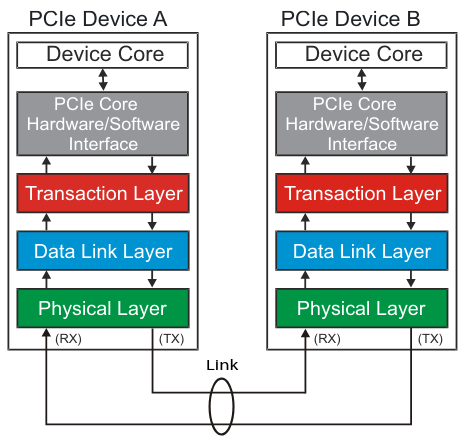
PCIe is divided into three main protocol layers, plus the device core at the top.
Each layer has a transmit path (TX) and a receive path (RX), and they work independently.
This means a device can send and receive data at the same time (full-duplex).
1️⃣ Device Core & Interface
- What it is: The actual function of the device (what it’s built to do).
- For a GPU → the graphics processor and its memory interface.
- For a NIC → the Ethernet MAC & PHY.
- For a switch → the internal routing fabric.
- Responsibilities:
- Talks to the Transaction Layer.
- Provides configuration space (up to 8 functions per endpoint).
- If it’s the Root Complex, it presents a virtual PCI bus 0 so that software can enumerate devices just like with legacy PCI.
2️⃣ Transaction Layer (TL)
- What it does: Creates and interprets Transaction Layer Packets (TLPs).
- Responsibilities:
- Packetization → wraps read/write requests, completions, and messages into TLPs.
- Ordering rules → ensures packets are delivered in the right order (unless Relaxed Ordering bit is set).
- Flow control → keeps track of available buffers so the link doesn’t overflow.
- QoS (Quality of Service) → can prioritize certain traffic (important in systems with mixed workloads).
- Think of it as: The “brains” of data transactions — knows what needs to be sent.
3️⃣ Data Link Layer (DLL)
- What it does: Adds reliability on top of the physical link.
- Responsibilities:
- Wraps TLPs into Data Link Layer Packets (DLLPs).
- Adds a sequence number + CRC to detect errors.
- Uses Ack/Nak protocol to confirm good packets and retransmit bad ones.
- Think of it as: The “guaranteed delivery” layer — makes sure every packet arrives correctly.
4️⃣ Physical Layer
-
What it does: Actually moves the bits across the PCIe lanes.
-
Transmit side:
- Takes DLLPs/TLPs, scrambles them to avoid long runs of 1s or 0s.
- Performs 8b/10b encoding (Gen1/Gen2) or 128b/130b encoding (Gen3+).
- Serializes data → converts from parallel bytes to a high-speed bit stream.
- Differentially drives signals on the lanes at the trained link speed.
-
Receive side:
- Deserializes the incoming bit stream.
- Recovers the clock using a CDR circuit.
- Decodes 8b/10b or 128b/130b symbols.
- De-scrambles and reassembles packets.
- Feeds the result to the DLL.
-
Extra job: Runs the LTSSM (Link Training and Status State Machine) to bring up the link, negotiate width/speed, and handle retraining if errors occur.
-
Think of it as: The “electrical” and “bit-level” layer — ensures that 1s and 0s get across reliably and in sync.
🧠 Why Layers Matter
- Design flexibility: Each layer is modular. You can update just one layer (e.g., switch to Gen5 physical layer) without redesigning the transaction layer logic.
- Troubleshooting: Engineers can debug where a problem occurs — transaction, link, or physical.
- Compatibility: Higher layers don’t care how the lower layers implement their work as long as the interface is followed.
📊 Quick Summary Table
| Layer | Main Job | Key Output |
|---|---|---|
| Device Core | Implements device function & config space | Requests to TL |
| Transaction | Creates TLPs, handles ordering/QoS/flow | TLPs |
| Data Link | Ensures reliable delivery (Ack/Nak) | DLLPs + TLPs |
| Physical | Serializes, encodes, transmits bits | Serial data stream |
Key Point: Every PCIe Interface Implements All Layers
Even if a device only forwards traffic (like a switch port), it still must have:
- Transaction Layer → to decode the packet headers, decide where to forward it.
- Data Link Layer → to ensure reliable delivery (Ack/Nak) across its link.
- Physical Layer → to actually serialize, transmit, and train the link.
So yes — switches implement all three layers per port.
Each port is basically its own PCIe endpoint/bridge, with its own state machine, buffers, and flow control logic.